Circuit diagram using only nands 3 input nand gate circuit diagram Nand gate circuit diagram circuits inputs power input electronic through pull down explanation button connected then
Logic NAND Gate Working Principle & Circuit Diagram
Nand gate schematic diagram
Digital logic nand gate(universal gate),its symbols & schematics
46+ circuit diagram of half adder using nand gateIntroduction to logic gates [diagram] circuit diagram nand gateCombinational mos logic circuits.
Nand gate diagram circuit ic 74ls00 pinout gates logic circuits chip not input circuitdigest working diagrams explanation electronic using limitationsNand gate circuit diagram and working explanation Logic nand gate working principle & circuit diagramNand gate diagram.

Nand gate layout
Nand gate diagramCmos nand gate circuit diagram Circuits not with nand gates diagram[diagram] circuit diagram nand gate.
Nand xor logic nor gates xnor circuit vhdl verify simulate input truth circuits tutorial engineersgarage scosche inverter inputs ckt combinedNand gate circuit diagram and working explanation Conversion of nand gate to basic gatesNand logic gates table paradoks circuitspedia logiczna gdzie filozoficzny logika bramka binarny czy.

Logic nand gate working principle & circuit diagram
Nand stick gate diagram cmos vlsi input mos logic circuit transistors schematic two figure circuits combinational euler given belowNand gates nor xnor circuit vhdl xor logic verify simulate circuits truth tutorial basic ckt Aman bharti's contentXnor gate circuit diagram using transistor.
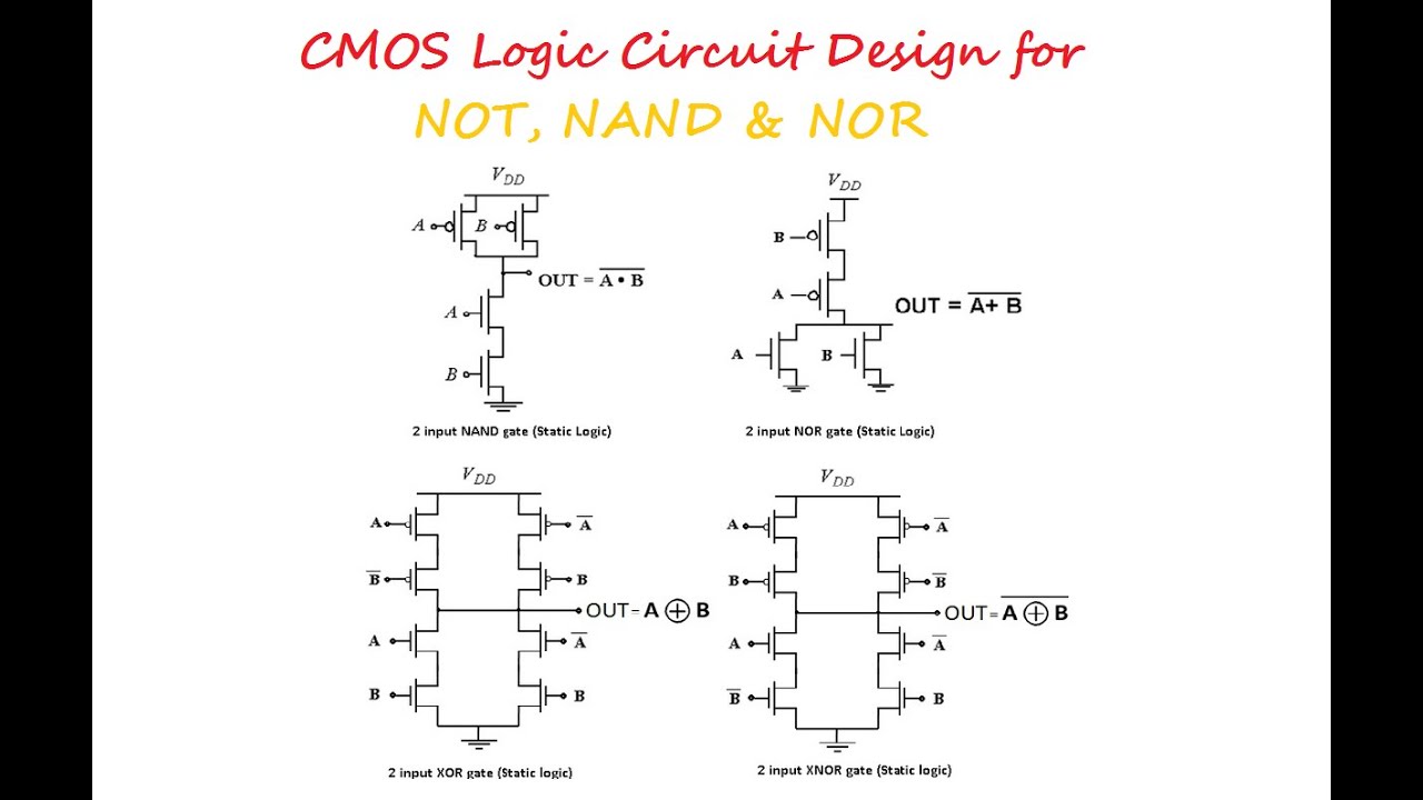
Vhdl tutorial – 5: design, simulate and verify nand, nor, xor and xnorVhdl tutorial – 5: design, simulate and verify nand, nor, xor and xnor Cmos logic circuit design for not, nand and nor gate.


![[DIAGRAM] Circuit Diagram Nand Gate - MYDIAGRAM.ONLINE](https://i2.wp.com/www.researchgate.net/profile/Jayanta_Pal10/publication/324926558/figure/download/fig2/AS:701079037677569@1544161676825/Schematic-diagram-of-implementation-of-basic-gates-using-NAND-gate.png)